CHS
CHS Walsun Mall
NEWS

More News
Share The Latest Information
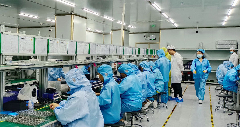
 Industry Dynamic +
  2023.11.07
Eye Diagram (Eye Diagram) can show the quality of digital signal transmission, often used in electronic equipment, chip serial digital signals or high-speed digital signals in the need to test and verify the occasion, in the final analysis, is the quality of the digital signal is a fast and very intuitive means of observation. In consumer electronics, high-speed signal transmission is often used within the chip and between the chip and the chip, if the corresponding signal quality is poor, it will lead to equipment instability, function execution error, or even failure. Eye diagram reflects the digital signal affected by the physical device, channel, engineers can quickly get the measured parameters of the signal in the product to be tested through the eye diagram, and can predict the problems that may occur in the field.
1, the formation of the eye diagram
For digital signals, its high level and low level changes can have a variety of sequence combinations. To 3 bits, for example, there can be 000-111 a total of 8 combinations, in the time domain will be enough of the above sequences according to a reference point alignment, and then superimposed on the waveform, the formation of the eye diagram, as shown in Figure 1. As in Figure 1, for the test instrument, the clock signal is first recovered from the signal to be tested, and then the eye diagram is superimposed according to the clock reference and finally displayed.

Figure 1: Formation of the eye diagram
2, the information contained in the eye diagram
For a real eye diagram, such as Figure 2, first of all we can see the average rise time (Rise Time), fall time (Fall Time), upswing (Overshoot), downswing (Undershoot), threshold level (Threshold/Crossing Percent), and other basic level shifting parameters of the digital waveform.

Figure 2. Level shift parameters
The signal can not be every time the voltage value of the high and low levels are kept exactly the same, also can not guarantee that every time the high and low levels of the rising edge, falling edge are in the same moment. As shown in Figure 3, due to the superposition of multiple signals, the signal line of the eye diagram becomes thicker and appears blurred (Blur). So the eye diagram also reflects the signal noise and jitter: in the vertical axis voltage axis, embodied in the voltage noise (Voltage Noise); in the horizontal axis time axis, embodied in the time domain jitter (Jitter).

Figure 3: Noise and jitter
Due to noise and jitter, the blank area on the eye diagram becomes smaller. As in Figure 4, based on the removal of jitter and noise, the distance of the blank area on the eye diagram on the horizontal axis is called the eye width, and when enough data are superimposed on the eye diagram, the eye width is a good reflection of the stabilisation time of the signals on the transmission line; similarly, the distance of the blank area on the vertical axis is called the eye height, and when enough data are superimposed on the eye diagram, the eye height is a good reflection of the stability time of the signal on the transmission line; similarly, the distance of the blank area on the eye diagram is called the eye height, and when enough data are superimposed on the eye diagram, the eye height is a good reflection of the stability time of the signal on the transmission line. Eye Height well reflects the noise tolerance of the signal on the transmission line, and at the same time, the place with the largest eye height in the eye diagram is the best judgement moment.
Figure 4. Eye height and width
Before and after the sampling of digital signals, there needs to be a certain amount of time to establish (Setup Time) and hold time (Hold Time), the digital signal should be kept stable during this period of time to ensure that the correct sampling, such as the blue part of Figure 5.1. As for the judgement of the input level, it is necessary that the voltage value of the high level is higher than the input high level VIH, and the voltage value of the low level is on the ground with the input low level VIL, as shown in the green part of Fig. 5.1. So, we can learn the earliest sampling moment and the latest sampling moment as shown in Figures 5.1 and 5.2.

Figure 5.1 Sampling and judgementa

Figure 5.2 Sampling and judgement b
At the best sampling moment, the sampling BER is the lowest, and as the sampling moment moves to both sides of the time axis, the BER keeps increasing, as shown in Figure 6. Therefore, engineering is also often drawn signal sampling period of the BER change curve, known as the bathtub curve (Bathtub Curve).

Figure 6. Bathtub Curve
In the actual test, in order to improve the efficiency of the test, often used to the method is Mask Testing, that is, according to the demand for signal transmission, in the eye diagram on the provisions of a region (such as Figure 7 in the diamond-shaped region), the requirements of the left and right signals all appear in this region outside, once the diamond-shaped region of the appearance of the signal, it is declared that the test has not been passed.

Figure 7. Mask Testing
Amplitude noise may cause vertical fluctuations in the voltage or power level of a logic '1' below the sample point, resulting in a logic '1' code incorrectly labelled as a logic '0' code, i.e., a miscode. Jitter describes the same effect, but it fluctuates horizontally. Jitter or timing noise may cause the edges of the code to fluctuate within the sample points in the horizontal direction, resulting in an error. In this sense, jitter is defined as a short-term variation of a digital signal from its ideal time position at an effective time point. Fluctuations in pulse voltage levels originate from unwanted amplitude modulation (AM). Similarly, timing fluctuations in conversion can be described as pulse phase fluctuations, unwanted phase modulation (PM), or phase noise.
Data communication and telecommunication technologies are not the same when it comes to timing of system devices. In synchronous systems, such as SONET/SDH, system devices are synchronised to a common system clock. When signals are transmitted over a network, jitter generated by different devices is propagated through the network, and jitter may increase indefinitely unless stringent requirements are placed on the jitter transmitted in the devices. In asynchronous systems such as Gigabit Ethernet, PCI Express, and Fibre Channel, device timing is provided by distributed clocks or from clocks reconstructed from data transitions. In this case, the jitter generated by the devices must be limited, but the jitter transferred from one device to another is less important. In either case, the bottom line is how well the system works, i.e., the BER.

Figure 8 Intersection of eye diagrams with large jitter, the histogram is the projection of a pixel wide block of intersections onto the time axis
The inherent jitter generated by the device is called jitter output. Its main sources can be divided into two: random jitter (RJ) and deterministic jitter (DJ). Jitter can be viewed as a timing change from an ideal timing position, logically transformed, as shown in the histogram in Figure 2. This distribution shows the ideal timing positions that are blurred by different sources of jitter. The jitter distribution is a convolution of the RJ and DJ probability density functions. Random jitter originates from various random processes, such as thermal and scatter-grain noise, which are assumed to adhere to a Gaussian distribution, as shown in Fig. 3a. Since the tails of the Gaussian distribution extend to infinity, the peak-to-peak values of RJ have no boundary, while the root mean square of RJ converges to the width of the Gaussian distribution.

Fig. 9 Example of a single point in time where a combination of jitter, sinusoidal periodic jitter and random jitter results in a BER
Ideal Transition Edge: Ideal transition edge
RJ Smeared Edge: RJ smeared edge
DJ Smeared Edge: DJ smeared edge
Deterministic jitter (DJ) includes duty cycle distortion (DCD), intercoder interference (ISI), sinusoidal or periodic jitter (PJ), and crosstalk. DCD arises from asymmetries in the clock cycle. ISI arises from variations in the edge response due to data correlation effects and dispersion, and PJ arises from electromagnetic pickup of cyclic sources, such as power feedthroughs. Crosstalk is caused by pickup of other signals. dj is characterised by its peak-to-peak values having upper and lower limits. dcd and isi are referred to as bounded correlation jitter; pj and crosstalk are referred to as uncorrelated bounded jitter; and rj is referred to as uncorrelated unbounded jitter.
Identifying the sources of different types of jitter can reduce problems at the design level because different devices generate jitter in different ways. For example, transmitters primarily generate RJ. most of the jitter generated by externally modulated laser transmitters is caused by random jitter in the laser and the master reference clock. In contrast, the vast majority of jitter generated by the receiver is DJ, which arises from factors such as AC coupling of the preamplifier and postamplifier connections that cause ISI. Directly modulated laser transmitters are affected by both RJ and DJ. The medium is used in two ways: the fibre adds DJ from dispersion and RJ from scattering; the conduction medium adds DJ from a finite bandwidth, with higher attenuation at high frequencies compared to low frequencies and multiple reflections.
Conclusion
High-speed Optical transceiver module, because of the device temperature characteristics, transmission skin effect, system bandwidth constraints, assembly parasitic parameters, transmission impedance mismatch, extinction ratio caused by a large number of deterministic jitter, electromagnetic interference, and so on, often make some products ineffective. The low saturation light power caused by the multi-line and APD temperature characteristics is the two failure modes when the high-Speed Optical transceiver module is tested.
Pre-aggravation and equalization of transmission signals is a common method for high-speed optical transceiver modules. Pre-aggravation and balanced treatment should be moderate. Moderate or not, can be measured by the optical receiving eye diagram and the sensitivity of light reception. This is the correct way to identify whether or not the emitter eye is qualified.

Subscribe to the newsletter
for all the latest updates.


2-5# Building, Tongfuyu Industrial Zone, Aiqun Road, Shiyan Street, Baoan District, Shenzhen. China
Copyright © 2023 Walsun Inc. All Rights Reserved.
Professional high-speed optical transceiver module overall solution provider